 '
'
The development of photovoltaic (PV) absorbers proper for thin films based devices has become fundamental in the last decades to increase the efficiency to cost ratio of solar energy and, mainly, to save raw materials. At a early stage, the research in thin film solar cells has been dominated by absorber materials based on CdTe and Cu(In,Ga)Se2. However, both the toxicity of cadmium and the scarce availability of In, Ga and Te lead towards the development of materials baased on earth-abundant and relatively harmless elements.
The most studied alternatives to CIGS are Cu2ZnSnS4 (CZTS) and Cu2ZnSnSe4 (CZTSe), where more abundant and less expensive elements like Zn and Sn are used in place of In and Ga. CZTS and CZTSe, whose most stable crystalline form is kesterite, have a direct band gap of 1.4-1.5 eV and 1.0 eV, respectively, as well as an absorption coefficient higher than 104 cm-1, which make them suitable for PV applications. They share similar structure with the chalcopyrite CuInS2 except that half of the In is replaced with Zn and another half with Sn.
Further alternatives are copper manganese tin sulfide (CMTS) and copper iron tin sulfide (CFTS), which both show an important advantage with respect to CZTS. As a matter of fact, not only the abundance in the Earth’s crust of Fe and Mn is orders of magnitude higher than that of Zn, but the amount of Zn annually produced is definetely lower than that of both Mn and Fe. Therefore, since Fe and Mn are definitely cheaper than Zn, optimized CMTS and CFTS could potentially provide Wp cost definitely lower than CZTS, which is crucial for thin film PV applications. Furthermore, they consist of non-toxic elements and show high absorption coefficient and direct band gap suitable for PV applications.
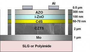
At MIB-SOLAR labs, CZTS thin films can be prepared both by sputtering and by a soft-chemical route. Using RF sputtering, tin, copper and zinc are deposited on a molydbenum thin layer and the CZTS phase is obtained by a thermal treatment of the stacked metals in sulfur vapours. To optimise the growth process, a comprehensive structural and spectroscopical characterization, including scanning electron microscopy coupled with energy dispersive spectroscopy (SEM/EDS), Raman spectroscopy, X-ray diffraction (XRD) and photoluminescence (PL) of the CZTS films was carried out. Electrical characterization of the solar cells demonstrates reproducible efficiency around 4%.
In the chemical method, the precursor solution is prepared by dissolving copper (II) acetate hydrate, tin (II) chloride dihydrate, zinc (II) acetate dihydrate and thiourea into DMSO. The solution is then drop-casted on Mo coated soda lime substrates. After 30 min of gelation process, a 10 min annealing in tubular oven under Ar atmosphere at 550 °C is performed. The drop-casting, gelation and annealing sequence is then repeated leading to a total film thickness around 2 μm. The so produced CZTS thin films are analyzed before and after each step with SEM/EDS, Raman, XRD and Photoluminescence. A similar procedure was used to obtain CFTS thin films with promising features.
Thin film solar cells based on both CZTSe grown by Politecnico di Milano and CMTS grown by RSE SpA are also prepared and tested at MIB-SOLAR labs. The relationships between material properties and PV device performance are established through a careful characterization of the absorber layers by Raman, XRD and Photoluminescence.
Research team: Prof. Simona Binetti (Full Professor), Prof. Maurizio Acciarri (Associate Professor), PhD Vanira Trifiletti (Assistant Professor), PhD Giorgio Tseberlidis (Assistant Professor), Fabio Butrichi (PhD student), Carla Gobbo (PhD student)
Selected pubblications:
- Gobbo, C., Di Palma, V., Trifiletti, V., Malerba, C., Valentini, M., Matacena, I., Daliento, S., Binetti, S., Acciarri, M., Tseberlidis, G. “Effect of the ZnSnO/AZO Interface on the Charge Extraction in Cd-Free Kesterite Solar Cells” Energies 2023, 16(10), 4137
- Trifiletti, V.; Frioni, L.; Tseberlidis, G.; Vitiello, E.; Danilson, M.; Grossberg, M.; Acciarri, M.; Binetti, S.; Marchionna, S., “Manganese-substituted kesterite thin-films for earth-abundant photovoltaic applications” Sol. Energy Mater Sol. Cells 2023, 254
- G. Tseberlidis, V. Di Palma, V. Trifiletti, L. Frioni, M. Valentini, C. Malerba, A. Mittiga, M. Acciarri, S.O. Binetti, “Titania as Buffer Layer for Cd-Free Kesterite Solar Cells” ACS Materials Lett. 2023, 5, 1, 219–224
- G. Tseberlidis, V. Trifiletti, E. Vitiello, A.H. Husien, L. Frioni, M. Da Lisca, J. Alvarez, M. Acciarri, S.O. Binetti, “Band-Gap Tuning Induced by Germanium Introduction in Solution-Processed Kesterite Thin Films” ACS Omega (2022), 7, 27, 23445–23456
- G. Tseberlidis, A.H. Husien, S. Riva, L. Frioni, A. Le Donne, M. Acciarri, S. Binetti “Semi-transparent Cu2ZnSnS4 solar cells by drop-casting of sol-gel ink” Solar Energy 224 134–141, (2021)
- C. Marchi, G. Panzeri, L. Pedrazzetti, M. I. Khalil, A. Lucotti, J. Parravicini, M. Acciarri, S. Binetti, L. Magagnin “One-step CZT electroplating from alkaline solution on flexible Mo foil for CZTS absorber“ Journal of Solid State Electrochemistry (2021)
- G. Tseberlidis, V. Trifiletti, A. Le Donne, L. Frioni, M. Acciarri and S. Binetti “Kesterite solar-cells by drop-casting of inorganic sol–gel inks” Solar Energy 208 (2020) 532–538
- V. Trifiletti, G. Tseberlidis, M. Colombo, A. Spinardi, S. Luong, M. Danilson, M. Grossberg, O. Fenwick and S. Binetti “Growth and Characterization of Cu2Zn1−xFexSnS4 Thin Films for Photovoltaic Applications” Materials 13 (2020) 1471
- Trifiletti, V., Mostoni, S., Butrichi, F., Acciarri, M., Binetti, S., & Scotti, R. “Study of Precursor‐Inks Designed for High‐Quality Cu2ZnSnS4 Films for Low‐Cost PV Application ” CHEMISTRY SELECT, 4(17), 4905-4912 2019.
- A. Le Donne, V. Trifiletti & S. Binetti “New Earth-Abundant Thin Film Solar Cells Based on Chalcogenides” Frontiers in Chemistry 7, 297 (2019)
- A. Le Donne, S. Marchionna, M. Acciarri, F. Cernuschi, S. Binetti,“Relevant efficiency enhancement of emerging Cu2MnSnS4 thin film solar cells by low temperature annealing” Solar Energy 149, 125-131 2017
- S. Marchionna, A. Le Donne, M. Merlini, S. Binetti, M. Acciarri, F. Cernuschi “Growth of Cu2MnSnS4 PV absorbers by sulfurization of evaporated precursors” Journal of Alloys and Compounds 693, 95-102 2017
- M. I. Khalil, R. Bernasconi, L. Pedrazzetti, A. Lucotti, A. Le Donne, S. Binetti, L. Magagnin “Co-Electrodeposition of Metallic Precursors for the Fabrication of CZTSe Thin Films Solar Cells on Flexible Mo Foil" Journal of The Electrochemical Society, 164 (6), D302-D306 2017
- M. Boshta, S. Binetti, A. Le Donne, M. Gomaa and M. Acciarri “A chemical deposition process for low-cost CZTS solar cell on flexible substrates” Materials Technology-Advanced Performance Materials 32(4), 245-249 2017
- M.I. Khalil, O. Atici, A. Lucotti, S. Binetti, A. Le Donne, L. Magagnin “CZTS absorber layer for thin film solar cells from electrodeposited metallic stacked precursors (Zn/Cu-Sn)” Applied Surface Science 379, 91–97 2016
- M. I. Khalil, R. Bernasconi, S. Ieffa, A. Lucotti, A. Le Donne, S. Binetti, L. Magagnin “Effect of co-electrodeposited Cu-Zn-Sn precursor compositions on sulfurized CZTS thin films for solar cell" ECS Transactions 64 (29), 33-41 2015
- A. Le Donne, S. Marchionna, P. Garattini, R.A. Mereu, M. Acciarri, S. Binetti “Effects of CdS Buffer Layers on Photoluminescence Properties of Cu2ZnSnS4 Solar Cells" International Journal of Photoenergy Article ID 583058, 8 pages 2015
- S. Tombolato, U. Berner, D. Colombara, D.Chrastina, M. Widenmeyer, S. Binetti and P.Dale “ Cu2ZnSnSe4 device obtained by formate chemistry for metallic precursor layer fabrication ” Solar Energy 116, 287–292 2015
- S. Marchionna, P. Garattini, A. Le Donne, M. Acciarri, S. Tombolato and S. Binetti Cu2ZnSnS4 solar cells grown by sulphurisation of sputtered metal precursors Thin Solid Films 542 2013 114–118.