 The study of phenomena based on heteroepitaxy is currently one of the hottest topics in semiconductor physics, because it provides insights and guidelines for the control of sophisticated structures at the nanometer scale. Among the various material systems, Si-Ge-Sn alloys have attracted a great attention in recent years since they display a wealth of interesting phenomena, e.g. a direct-to-indirect bandgap transition was experimentally demonstrated, while calculations have predicted a correlation-driven transition between metallic and Mott-insulating surfaces and even a superconductive phase upon doping.
In the foreseeable future, the fundamental research carried out within this project on group IV semiconductors might unfold the remarkable properties of this material platform. Specifically, from a technological point of view the unmatched properties of SiGeSn micro and nanostructured alloys can boast them as an excellence candidate to meet energy efficiency requirements in line with the EC directives. The latter set an ambitious road map with an important target for the introduction of renewable energy in gross consumption.
Our research explores phenomena that interlink the optical and electronical degrees of freedom: the key focus of thin film photovoltaics. A unique approach based on nanostructured Si-Ge-Sn alloys can be the result of a robust research in the field of carrier dynamics and structural properties. This goal requires to break down barriers and bring diverse disciplines together, opening new research paths in renewable energies. The intriguing aspect of controlling scattering and recombination channels by precisely tuning structural and electronic properties of nanostructured semiconductors harnesses creative and unprecedented strategies to overcome research roadblocks towards the full exploitation of group IV photovoltaics.
The objective of our research is the control and manipulation of optical phenomena in SiGeSn-based alloys. This will be accomplished via the following steps: (i) Design of nanostructured group IV-based alloys with well-controlled and desired properties and (ii) Detailed investigation of electronic properties of the developed nanostructures.
Another technologically relevant material platform is that composed of III-V-on-Ge heterostructures. These show great promise for achieving high efficiency multijunction photovoltaic cells, allowing to tackle the economic and environmental cost of renewable energies. Bandgap engineering can be used to fine-tune the spectral response of the solar cell maximizing its efficiency, with special interest in energies around 1 eV.
One of the possible ways to engineer the bandgap of these heterostructures is to exploit lattice-mismatched (metamorphic) layers with varying composition. The understanding of lattice mismatch in multilayer heterostructures and the possibility for its control is critical to avoid nucleation of extended defects and resulting performance loss.
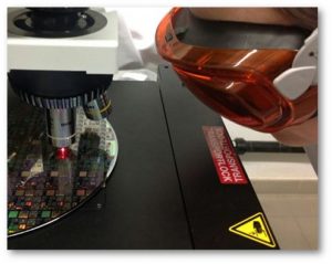
Our research is focused on the characterization of metamorphic III-V-on-Ge layers through optical techniques, with the goal of optimizing the strain and the energy gap while minimizing the defect density for the application to high efficiency multijunction photovoltaic cells. This research is conducted as part of the the CANVAS project, funded by the Italian Ministry of the Environment and the Energy Security.
Research team: Prof. Emiliano Bonera (Associate Professor), Prof. Fabio Pezzoli (Associate Professor), Dr. Jacopo Pedrini (assistant professor), Eleonora Bonaventura (postdoc), Ian Colombo (PhD student), Stefano Achilli (PhD student), Riccardo Nardin (PhD student)
Selected publications:
Pezzoli, F; Giorgioni, A; Patchett, D; Myronov, M; Temperature-Dependent Photoluminescence Characteristics of GeSn Epitaxial Layers; ACS PHOTONICS 3 (11) (2016) 2004-2009

 '
'